
Adam Nance
Sr. Printed Circuit Board Designer at Optimum Design Associates
 Email:
a****@optimumdesign.com
Email:
a****@optimumdesign.com
 Phone Number: (***)-***-****
Designed complex, high-speed printed circuit boards for the Aerospace, Defense, Satellite, and Communication industries using the latest Expedition and Altium toolsets.
Read More
 Profile Privacy
-
Share Profile


OPTIMUM DESIGN ASSOCIATES
-
 Headquarters: 1807 Santa Rita Rd, Pleasanton, California, 94566, United States
-
 Industry Consumer Electronics
-
 Website optimumdesign.com
-
HQ Phone 92********
-
 Description
Optimum Design is one of the United States most sophisticated mid-volume contract manufacturers and features the most honored PCB layout team in the world. Optimum delivers tier one capabilit...Read More

-
 Employees 51-200
-
 Revenue 25 Million to 50 Million
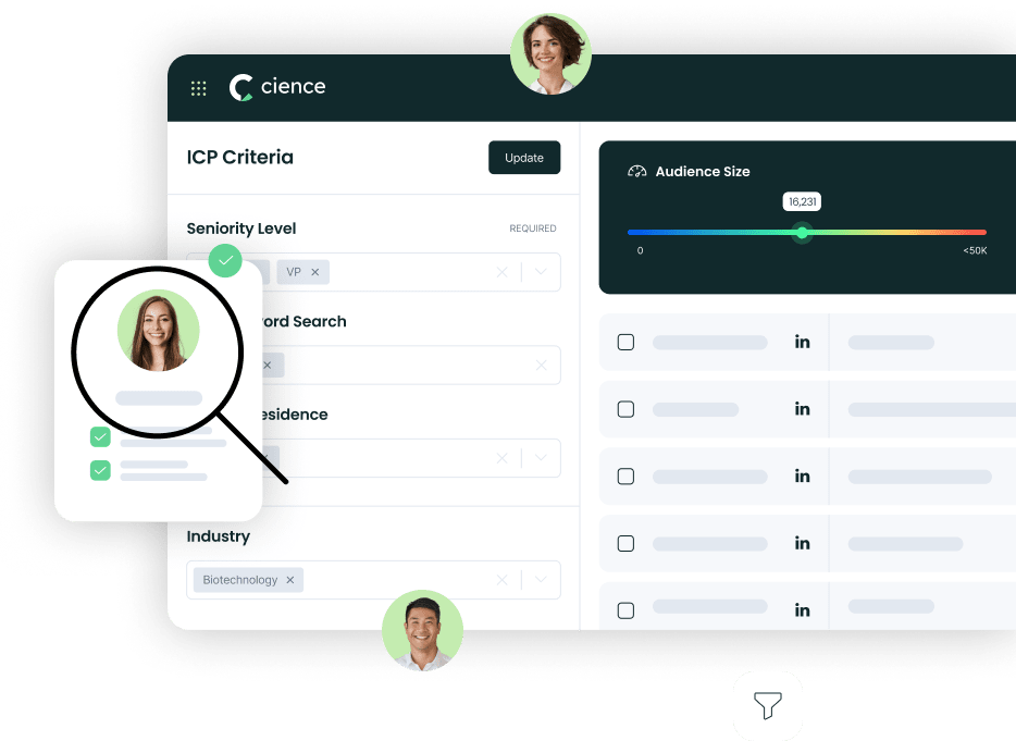
Sign in to CIENCE GO Data to uncover contact details
![]() Free credits every month
Free credits every month
Optimum Design Associates Org Chart and Mapping
Frequently Asked Questions Regarding Adam Nance
Answer: Adam Nance works for Optimum Design Associates as Sr. Printed Circuit Board Designer
Answer: Adam Nance’s role in Optimum Design Associates is Sr. Printed Circuit Board Designer
Answer: Adam Nance's email address is a***@gmail.com
Answer: Adam Nance's business email address is a****@optimumdesign.com
Answer: Adam Nance’s direct phone number is (***)-***-****
Answer: Adam Nance works in the industry of: Consumer Electronics
Answer: Adam Nance is the current Sr. Printed Circuit Board Designer at Optimum Design Associates.... Read More
Answer: Adam Nance works Optimum Design Associates located at 1807 Santa Rita Rd, Pleasanton, California, 94566, United States
Answer: Optimum Design Associates's Sr. Printed Circuit Board Designer is Adam Nance
Answer: Adam Nance contact details:
- Phone number : (***)-***-****
- Email : a****@optimumdesign.com
Premium Sales Data for Prospecting
-

Sales data across over 200M records
-
Up-to-date records (less decayed data)
-
Accurate Email Lists (real-world tested)
-
Powerful search engine and intuitive interface
Powered by
Sign in to CIENCE GO Data to uncover contact details
![]() Free credits every month
Free credits every month