 Phone Number: +19*********
Who is S-CUBED
Over a 25 year period, our solutions to semiconductor lithography processing for wafer level chip scale packaging (WLCSP), FEOL lithography, and 3/5 lithography requirements have evolved ...
Read More
-
 Headquarters: Montville, New Jersey, United States
-
 Date Founded: 1994
-
 Employees: 11-50
-
 Active Tech Stack: See technologies
![]() Industry: Semiconductors
Industry: Semiconductors
S-Cubed Org Chart and Mapping


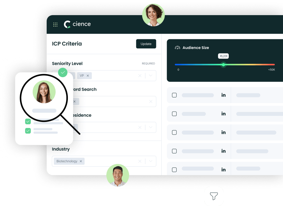
Sign in to CIENCE GO Data to uncover contact details
![]() Free credits every month
Free credits every month
Frequently Asked Questions Regarding S-Cubed
Answer: S-Cubed's headquarters are located at Montville, New Jersey, United States
Answer: S-Cubed's phone number is +19*********
Answer: S-Cubed's official website is https://s-cubed.com
Answer: S-Cubed has 11-50 employees
Answer: S-Cubed is in Semiconductors
Answer: S-Cubed contact info: Phone number: +19********* Website: https://s-cubed.com
Answer: Over a 25 year period, our solutions to semiconductor lithography processing for wafer level chip scale packaging (WLCSP), FEOL lithography, and 3/5 lithography requirements have evolved to provide more reliability and versatility at a lower cost than any other process solution provider in the industry. Deployed at fabs worldwide, our semiconductor equipment reliably bakes, coats, and develops millions of wafers every year.
Premium Sales Data for Prospecting
-

Sales data across over 200M records
-
Up-to-date records (less decayed data)
-
Accurate Email Lists (real-world tested)
-
Powerful search engine and intuitive interface
Powered by
Sign in to CIENCE GO Data to uncover contact details
![]() Free credits every month
Free credits every month